Micron Drops 4F² DRAM Plans, Betting on 6F² Scaling and 3D Memory
Micron says 4F² cells add cost without improving practical density, and plans to keep scaling 6F² DRAM while developing a 3D successor.
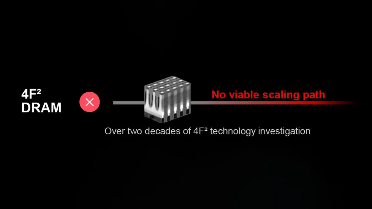
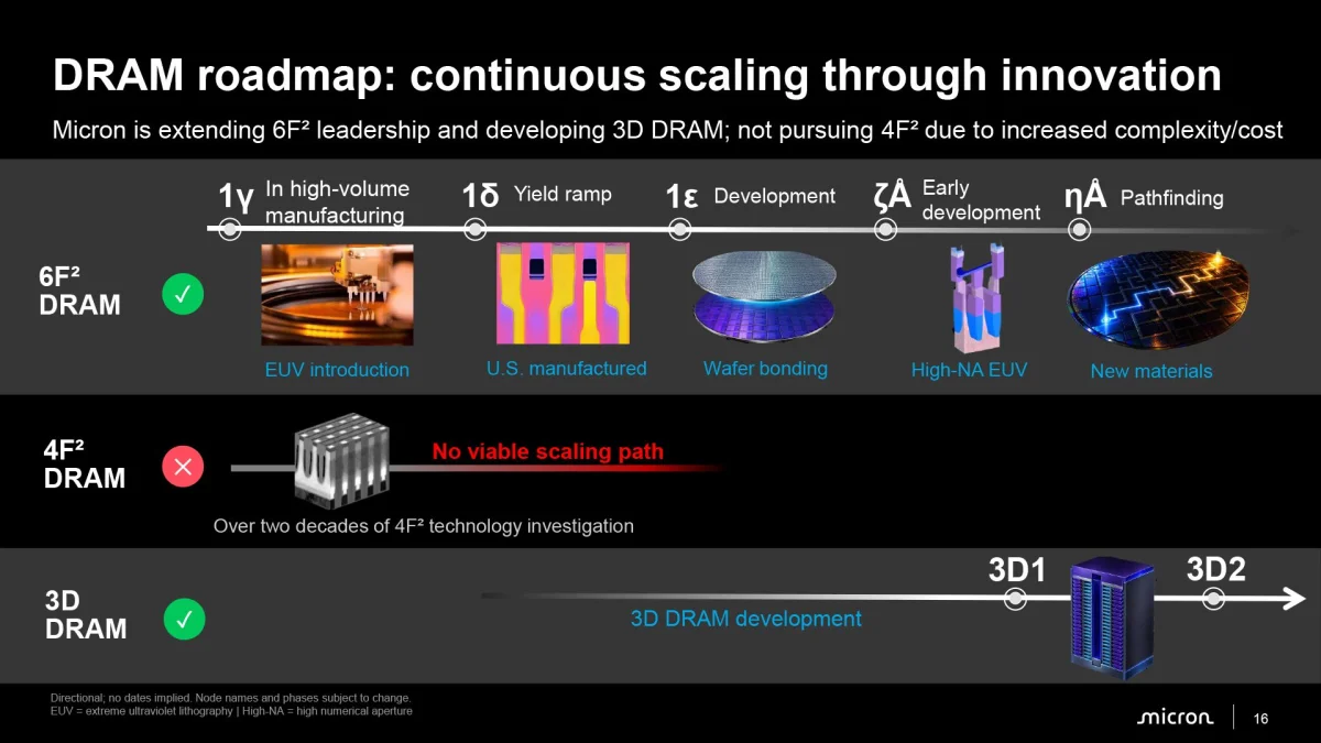
Micron has decided that shrinking DRAM transistors into a 4F² cell layout won’t deliver enough practical density to justify its added manufacturing complexity. After studying the design for roughly two decades and building experimental devices, the company plans to keep scaling conventional 6F² DRAM and develop 3D memory for the longer term.
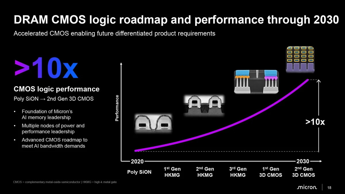
The decision sets Micron apart from Samsung and SK hynix, which, according to TechInsights, still include 4F² cells in their roadmaps. It also fits a pattern in Micron’s technology choices: the company has previously delayed adopting EUV lithography while maintaining competitive cost and performance. That history doesn’t prove the 4F² decision will produce the same result, but it shows Micron is willing to pursue a different manufacturing path from its rivals.
Why a smaller cell may not mean denser memory
The labels describe the area assigned to a DRAM cell in relation to the minimum lithographic feature size, or F. A 6F² cell occupies six times F squared; a 4F² cell occupies four times F squared. If all other dimensions stayed equal, that change would cut cell area by about one-third and could theoretically allow 50% more cells in the same area.
That arithmetic describes the transistor layout, though, not necessarily the size of the complete memory cell. Every DRAM cell also needs a capacitor to store data. Micron CTO Scott DeBoer argues that capacitor dimensions and spacing set the practical cell density: the transistors still have to fit beneath the capacitor layout. Making the transistor footprint smaller therefore doesn’t guarantee that more complete cells will fit on a wafer.
DeBoer said that capacitor pitch, size and dimensions determine DRAM bit density, rather than whether the transistor structure is called 4F², 6F² or 8F². His criticism is that the smaller nominal cell can sound like a direct density improvement even when the capacitor arrangement prevents that gain from carrying through to the finished device.
Micron also says implementing 4F² adds process complexity and cost. The company’s case, then, rests on two linked points: the architecture may not shrink the full cell enough to raise density, and it demands extra manufacturing work to get there. The source provides no cost estimate or direct comparison of production yields, so the size of those tradeoffs remains unspecified.
Micron’s alternative: keep shrinking 6F²
Micron intends to raise bit density through further reductions in capacitor pitch and process dimensions while retaining the 6F² architecture. The company says advanced lithography, new materials and wafer bonding can extend planar DRAM scaling for several more generations.
One upcoming step is the 1δ process, which Micron expects to enter volume production in the second half of 2027. The company projects a mid-20% improvement in bit density over its predecessor. That figure is a stated target; the source gives no details about product capacity, cost per bit or measured production results.
Micron also plans to use High-NA EUV lithography in future DRAM generations. DeBoer’s comments suggest the company sees a choice between adding the complications of 4F² and continuing to invest in more advanced process technologies. Micron hasn’t described the specific physical limits it sees in 4F², but says the architecture lacks a sustainable scaling path beyond a certain point.
DeBoer acknowledged that 4F² can be built, particularly by returning to earlier process generations. The problem, in Micron’s account, is extending it as dimensions shrink: complexity and cost rise, while fundamental scaling constraints eventually become more significant. That makes the architecture look like an intermediate step with limited long-term value for the company.
3D DRAM is the longer-term target
Micron’s preferred longer-term direction is 3D DRAM, which would increase density by stacking memory cells vertically instead of relying only on smaller lateral dimensions. The company is developing multiple generations of 3D DRAM production nodes alongside its next planar processes.
Micron hasn’t disclosed when 3D DRAM will reach commercial production. DeBoer said the transition will depend on whether the approach offers the right balance of density, manufacturing complexity and cost. Until then, the company’s stated plan is to extend 6F² DRAM through process improvements.
For memory buyers and developers, the announcement changes expectations about Micron’s technology path, but it doesn’t establish which supplier will achieve better density or economics. Samsung and SK hynix continue to list 4F² in their plans, while Micron says capacitor constraints make the cell-area comparison a poor guide to practical density. The useful test will be how each approach performs in manufacturable products, and whether 3D DRAM reaches Micron’s cost and density targets.