Intel Starts Fab 62 Tool Installation as Ohio One Construction Advances
Fab 62 is targeting operations by late 2028, while Intel reports High-NA EUV use in manufacturing and another construction milestone in Ohio.
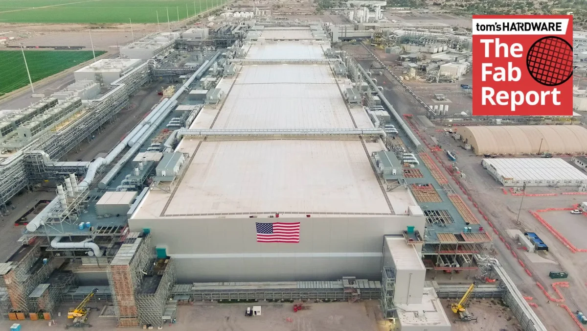
Intel’s Arizona expansion has moved from building construction to equipment installation: production tools are now going into Fab 62, which the company expects to become operational before the end of 2028. The milestone gives a clearer view of the facility’s progress, but key planning details remain undisclosed, including its process nodes, capacity and start date for high-volume output.
The update also links three parts of Intel’s manufacturing effort: a new Arizona fab, continued construction in Ohio, and the use of High-NA EUV lithography in high-volume manufacturing. Together, they show activity across facilities at different stages. They don’t yet provide a full picture of how much additional chip output those projects will deliver or when it will arrive.
“There is an important difference between technologies made in America and technologies that are truly American-made,” wrote Naga Chandrasekaran, Intel Foundry executive vice president and chief technology and operations officer. “The difference lies in the research and development process that transforms ideas into manufacturable technologies.”
Fab 62 moves into equipment installation
Intel had completed the shell of Fab 62 before beginning the current tool installation work. The facility will be the sixth high-volume semiconductor fab at the company’s Ocotillo campus in Arizona, a long-running production site that already includes advanced chip manufacturing and packaging, assembly and testing operations.
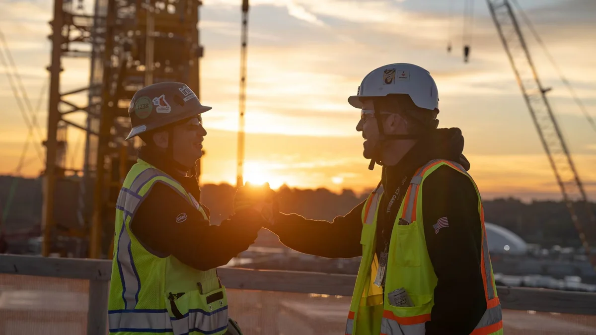
Tool installation is a substantial step beyond completing the building, but it doesn’t by itself establish when the fab will begin producing chips at scale. Intel has set a target for the facility to become operational before the end of 2028, without specifying a date for high-volume manufacturing. It also hasn’t disclosed Fab 62’s planned wafer capacity or the remaining capital spending needed to complete it.
The process assignment is open as well. Intel originally described Fab 52 and Fab 62 as facilities for advanced technologies including Intel 20A and 18A. It later designated Fab 52 for Intel 18A production; Fab 62 has no confirmed node assignment.
Based on Intel’s process roadmap, Fab 62 could be capable of producing chips on Intel 18A, 18A-P or 14A. Intel already makes 18A chips at neighboring Fab 52, leaving the new building as a possible source of added capacity for that process or a future site for 14A. Those are possibilities, not a confirmed production plan. The choice will affect how the facility fits into Intel’s manufacturing roadmap, but the company hasn’t shared enough detail to judge its expected output.
High-NA EUV enters high-volume manufacturing
Intel also confirmed that it has integrated High-NA EUV lithography into high-volume manufacturing. The company previously installed a commercial High-NA EUV scanner at its D1X facility near Hillsboro, Oregon. That site develops advanced logic processes and starts production of newer processors, making it a place to work through the requirements of a new lithography system.
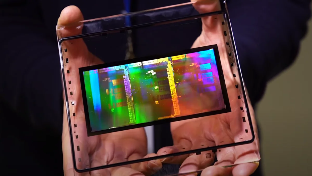
Intel says High-NA EUV has been used to produce selected tiles for Panther Lake processors and other chips. The update establishes that the equipment has a role in manufacturing, though it doesn’t describe how broadly the technology is being used or quantify any resulting improvement in performance, cost or production efficiency.
There’s also a gap between using a new scanner and proving that it changes what a chipmaker can produce. The source reports that High-NA EUV may currently be patterning circuits also made with Low-NA EUV tools. Intel hasn’t explicitly confirmed that comparison, and its update doesn’t say whether the newer equipment enables smaller features, reduces process steps or improves yields in this use. For now, its manufacturing use is a notable process milestone, while the practical gains remain unclear.
Ohio construction advances without a production date
At Intel’s Ohio One complex in New Albany, workers installed the first major structural truss for the site’s first semiconductor fab. The work marks progress on the building, but Intel didn’t provide a revised construction schedule or say when the fab is expected to start operations.
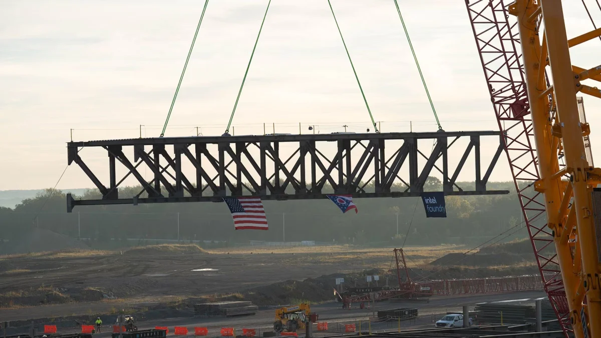
The process technology and planned capacity for the Ohio facility also remain undisclosed. That leaves an important distinction between visible construction progress and a firm forecast for chip supply: the truss indicates that work is advancing, but it doesn’t answer when Ohio One will contribute output or what kinds of chips it will make.
Manufacturing depends on more than wafer fabs
Intel’s U.S. operations also include research and development, advanced packaging, assembly, testing and photomask production. Oregon is its main center for advanced logic and 3D interconnect research. Arizona hosts advanced packaging research and development alongside assembly and testing. In New Mexico, Intel makes multi-chiplet processors using packaging approaches that include EMIB, as well as newer EMIB-T and Foveros technologies.
The company has also started work on a photomask manufacturing facility in Santa Clara, California. Photomasks are part of the chipmaking supply chain, and producing them alongside process development and wafer fabrication can add domestic capability. Intel’s account presents this combination as a distinguishing feature of its U.S. operations. The company still relies on tools from Europe and materials from Japan, so its supply chain is not entirely domestic.
Intel says its U.S. operations work with more than 4,500 suppliers across 49 states and that annual domestic spending exceeds $29 billion. Those figures give a sense of the supply network surrounding its facilities, though they don’t indicate how much production capacity the new projects will add.
The most concrete near-term signal is Fab 62’s transition to tool installation, alongside a stated target for operations by late 2028. Ohio One has reached a construction milestone without a corresponding schedule, and High-NA EUV has entered manufacturing without published figures on its effects. The next useful measure will be whether Intel supplies dates, process assignments and capacity details that connect these investments to actual chip output.